CS253-Note
Lecture-1 CPU#
Types of computer#
Harvard:
Memory to store instructions (operators) is separate to the memory used for data (operands). 存储指令(操作符)的内存与用于数据(操作数)的内存是分开的。
Von Neumann:
There is only one memory used for both data and instructions. Looking at bytes in memory it would difficult to tell with certainty which stores code and which stores data. 只有一个内存用于数据和指令。 查看内存中的字节,很难确定哪些存储代码,哪些存储数据。
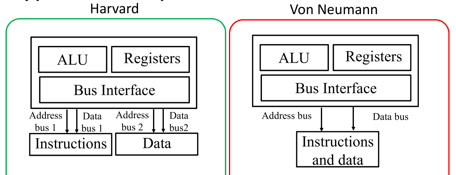
ALU: Arithmetic Logic Unit 算术逻辑单元 Registers:寄存器 Bus Interface: 总线接口 Instructions: 指示集 Data: 数据
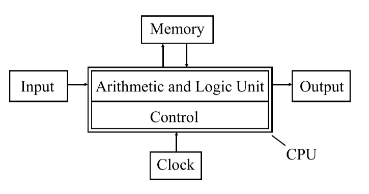
Organisation of a von Neumann digital electronic computer#
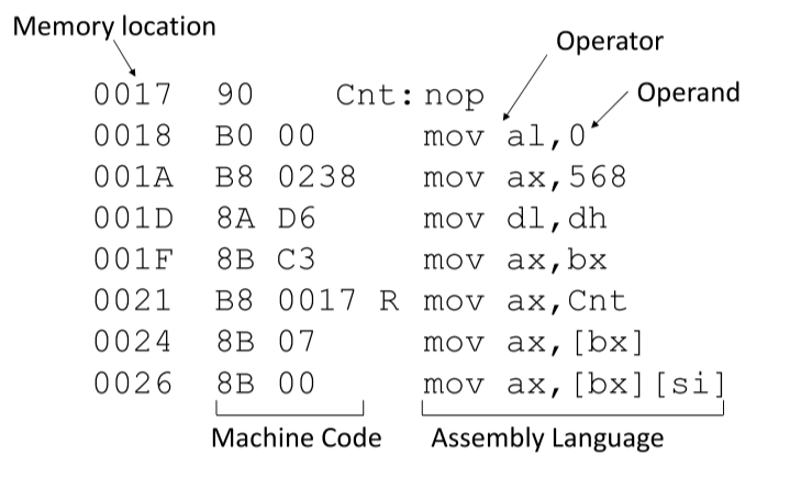
Assembly Language#
Organisation of a digital computer#
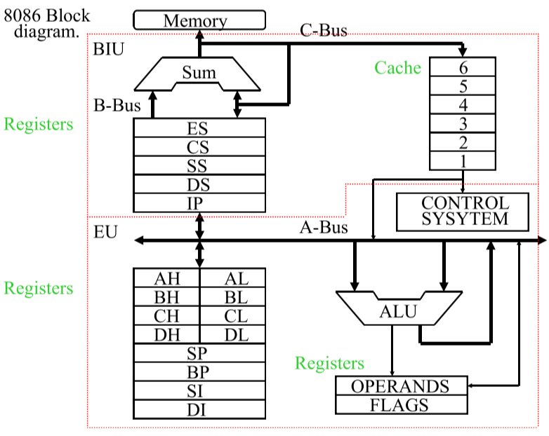
The CPU has two main function blocks
BIU: Bus Interface Unit BIU: 总线接口单元 The BIU sends outs addresses fetches instructions from memory and reads and writes to ports and to memory. BIU 发送出地址,从内存中获取指令并读取和写入端口和内存。
EU: Execution Unit The EU instructs the BIU where to fetch instructions, it decodes instructions and executes instructions. 执行单元 EU 指示 BIU 从何处获取指令,它对指令进行解码并执行指令。 The EU contains both the ALU and Control Circuitry. EU 包含 ALU 和控制电路。
The A-Bus, B-Bus and C-Bus are high speed data paths contained within the Microprocessor itself. A-Bus、B-Bus 和 C-Bus 是包含在微处理器本身内的高速数据路径。
Control Circuits (EU)#
The control unit fetches instructions from the queue. The queue is a first in first out store of 6 bytes. 控制单元从队列中获取指令。该队列是一个6字节的先入先出存储器。 The store is kept full by the BIU. This means that main memory is not accessed for each byte of each instruction. The technique is known as pipleling. 存储器由BIU保持完整。这意味着每条指令的每个字节都不需要访问主内存。这种技术被称为 "流水线"。 Some instructions such as conditional jumps and call to subroutines can not be pipelined (more later). 一些指令,如条件性跳转和调用子程序,不能进行流水线处理 (后面会详细介绍)。
The ALU (EU)#
The ALU in the 8086 can ADD, Subtract, AND, OR, XOR, increment, decrement, complement and shift 16-bit binary numbers.
后面的一部分关于数电的看不懂#
Lecture-2 Assembly Language#
General Purpose Registers#
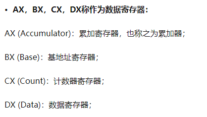
The 8086 has eight general purpose registers. As a programmer you can think of them as eight variables. Al is the accumulator and there are more instructions associated with it than any other register. Each register is eight bits wide. However some instructions can uses registers in pairs, giving 16 bit operation. 8086有八个通用的寄存器。作为一个程序员,你可以把它们想象成八个变量。Al是累加器,与它相关的指令比任何其他寄存器都多。每个寄存器都是8位宽。然而,有些指令可以成对使用寄存器,提供16位的操作。
Lecture-3 Assembly Language#
Addressing Modes#
The different ways the processor can access memory are known as addressing modes. 处理器访问内存的不同方式称为寻址模式。 $$ mov al,\dots or mov \dots,al $$
-
* Immediate addressing 立即寻址,直接将常数传给寄存器就是一种直接寻址 $$ mov ax,568 $$
-
* Register addressing 寄存器寻址 The contents of register
axis copied intobx. $$ mov bx,ax $$ The contents of registerbhis copied intodl. $$ mov dl,bh $$ -
* Direct addressing 直接寻址
The contents of the memory location DS:Count is copied into ax .
$$
mov ax,Count
$$
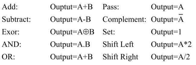
- * Register Indirect Addressing 寄存器直接寻址
在这种寻址模式中,16 位偏移地址包含在 16 位寄存器(索引寄存器、BX、BP、SI 或 DI)中。 段寄存器与偏移寄存器相结合,在内存中定位要访问的地址。
| Text Only | |
|---|---|
寄存器间接寻址是一种以与高级语言中的数组类似的方式访问内存的方法。
mov ax,[bx] 将数据段中寄存器 bx 指向的内存位置的内容移动到寄存器 ax 中
mov [bx], ax 将寄存器 ax 中存储的值放入数据段中 bx 所指向的位置。
- Register Indirect with Displacement 使用基址和索引寄存器间接注册
这个模式和之前的模式很相似,偏移量是通过两个16位寄存器相加得到的,然后再和相关的段寄存器组合结果
-
Register Indirect with base and register
-
Register Indirect with base and index and constant
最后三个没打星号不看了
Lecture-4 Assembly Language#
Types of Instruction#
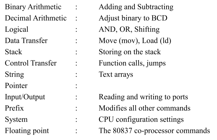
Binary Arithmetic#
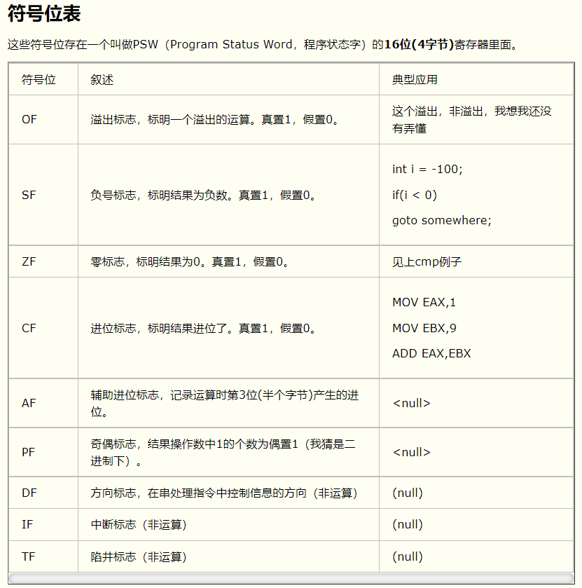
ADD 加 SUB 减 ADC Add with carry (就是在加的基础上再加上 CF Carry Flag)
CMP 比较 将两个数相减得出结果,若结果为 0,则证明两数相等,将 1 存入 ZF
INC increase DEC decrease
DIV 除
MUL 乘 Note: only one operand, always in AX
DIV 10 ;AX=AX/10 MUL BX ;AX = AX*BX
Logical Instructions#
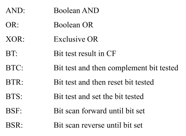
OR Function often used to convert BCD to ASCII
Logical Shift#
汇编移位运算 - 明亮先森 - 博客园 (cnblogs.com)
SHL 逻辑左移(无符号数) SHL 1 or SHL cl
运算规则 向左移动 低位补 0 高位移至 CF
注:移动 n 位相当于无符号数乘 2 的 n 方
SHR 逻辑右移(无符号数) SHR 1 or SHR cl
运算规则 向右移动 高位补 0 低位移至 CF
注:移动 n 位相当于无符号数除 2 的 n 方
SAL 算数左移(有符号数) SAL 1 or SAL cl
运算规则 向左移动 低位补 0 高位移至 CF
注:移动 n 位相当于有符号数乘 2 的 n 方
SAR 算数右移(有符号数) SAR 1 or SAR cl
运算规则 向右移动 高位补最高位 低位移至 CF
注: 移动 n 位相当于有符号数除 2 的 n 方
第七位补原符号位,即和原第七位相同
Control Transfer#
Branch Control Transfer Functions#
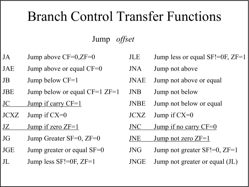
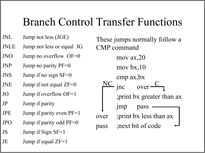
常与 CMP 指令一起使用
CMP 比较 将两个数相减得出结果,若结果为 0,则证明两数相等,将 1 存入 ZF
JC Jump if carry CF = 1 JNC Jump if not carry CF = 0
JZ Jump if zero ZF = 1 JNE Jump not zero ZF = 0
JE SOME_WHERE ;检查ZF,为1就跳 JNE SOME_WHERE ;检查ZF,为0就跳
汇编条件判断整理(JCC,CMP/TEST的实现) - VinoZhu - 博客园 (cnblogs.com)
Lecture-5 Assemply Language(Data Types, Intergers, Real and String)#
Lecture-6 Assembly Language(Floating Point, 8087)#
Lecture-7 Semiconductors PN Junction diode#
Lecture-8 Transistors and FETS#
Lecture-9 Digital I/O#
Interrupts#
Most advanced microprocessors allow normal linear program operation to be interrupted by some external signal or by a special instruction in the program. 大多数先进的微处理器允许正常的线性程序操作被一些外部信号或程序中的特殊指令中断。
When Interrupted the microprocessor,
- suspends execution of the main program,
- calls a procedure which services the interrupt (interrupt handler or interrupt service routine),
- returns control to the mainline program.
Interrputs Type#
The three types of Interrupt 8086:
- Hardware Interrupts
An external signal applied to the INTR (interrupt) pin or NMI (interrupt) pin of the processor causes an interrupt. 施加到处理器的 INTR(中断)引脚或 NMI(中断)引脚的外部信号会导致中断。
- Exception Interrupts
Triggered by internal errors such as divide by zero, normally to print an error message. 由内部错误触发,例如除以零,通常打印错误消息。
- Software Interrupts
Caused by the execution of an assembly language INT command. Simply a call to a function in BIOS. 由执行汇编语言 INT 命令引起。只需调用 BIOS 中的函数。
Interrupt Processing Sequence#
Hardware requests service routine by bringing IRQx low. 硬件通过降低 IRQx 来请求服务程序。
The 8259A signals to CPU via INTR line. 8259A 通过 INTR 线向 CPU 发送信号。
The CPU responds with Interrupt Acknowledge signal (INTA). CPU 以中断确认信号 (INTA) 进行响应。
The Acknowledge signal causes the 8259A to place the interrupt number (0-255) on the data bus. Acknowledge 信号使 8259A 将中断号 (0-255) 放置在数据总线上。
CPU reads the data. CPU 读取数据。
CPU hardware related registers onto the stack, including current CS:IP,SP and Flags. CPU 硬件相关寄存器入栈,包括当前 CS:IP,SP 和 Flags。
CPU multiplies Interrupt No.(Type) by 4 and looks up the jump address in the vector table. CS and IP are changed. CPU 将中断号(类型)乘以 4 并在向量表中查找跳转地址。CS 和 IP 变化。
Execution of the interrupt service routine continues until IRET. 中断服务程序的执行一直持续到 IRET。
IRET registers to be restored to their former values. IRET 寄存器恢复到它们以前的值。
CS and IP are restored and the main program continues. CS和IP恢复,主程序继续。
Lecture-10 MASM Code for Interrupts#
Lecture-11 Memory Hierarchy & Dynamic and Static RAM#
Main Memory#
Static RAM#
- Construction based on Flip Flops 基于触发器的结构
- Each memory cell uses up a lot of real estate 每个存储单元都占用了大量的空间
- Memory is volatile, but does not need refreshing 内存是不稳定的,但不需要刷新
- Much faster than Dynamic Ram, used for caches, 10nS 比动态RAM快得多,用于缓存,10nS
Dynamic RAM#
- Construction based on charge stored on the gate of a FET. 基于存储在 FET 栅极上的电荷的构造。
- Much higher densities possible (larger memory) 可能的密度更高(更大的内存)
- Lower Cost 更低的开销
- But requires extra refresh control signal. 但需要额外的刷新控制信号。
- Typically 60nS, no dissipation when not accessed. 通常为 60nS,未访问时无耗散。
Lecture-12 Memory Management Cache strategies#
Lecture-13 The hard disk CD-ROM#
Disk Layout#
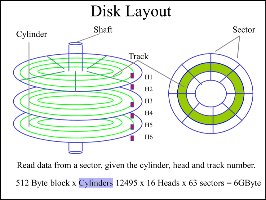
512 Byte block x Cylinders 12495 x 16 Heads x 63 sectors = 6GByte
Lecture-14 CISC/RISC Vector Processors Parallel Processors#
Lecture-15 Buses#
Doc-Flash RAM and FPGA#
Solid State Drive(SSD)#
Flash-based media are based on a silicon substrate and therefore are known as solid-state devices. They are widely used in both consumer electronics and large data storage systems.
There are three SSD form factors widely used in personal computers:
- SSDs that fit into the same slots used by traditional hard disk drives (HDDs) and uses the standard HDD interfaces such as SATA or SCSI.
- Solid-state cards built on a printed circuit board and use a standard I/O interface, such as Peripheral Component Interconnect Express (PCIe).
- Solid-state modules that fit in a dual inline memory module (DIMM) or small outline dual inline memory module using a standard HDD interface, such as SATA.
An additional subcategory is a hybrid hard drive that combines a conventional HDD with a NAND flash module. The flash part provides very fast I/O while the HDD part can store a large amount of data.
Flash memory#
Here are some advantages of flash memory:
-
Flash is the least expensive form of semiconductor memory.
-
Unlike dynamic random access memory (DRAM) and static RAM (SRAM), flash memory is non-volatile, offers lower power consumption and can be erased in large blocks.
-
NOR flash offers increased random read speeds, while NAND flash is fast with serial reads and writes.
-
An SSD with NAND flash memory chips delivers significantly higher performance than traditional storage media, such as HDDs, compact discs and tape.
-
Flash drives are more reliable than HDDs as they have no moving parts.
-
Enterprise storage systems equipped with flash drives are capable of low latency, which is measured in microseconds or milliseconds.
The major disadvantages of flash memory are:
-
SSDs are much more expensive compared to equivalent HDDs.
-
Also, at the present, HDDs have a larger capacity. HDD of 12 TB can be obtained, but the largest SSD has a capacity of only 2 TB.
-
The wear-out mechanism where memory cells can fail with excessively high numbers of program/erase cycles, which eventually break down the oxide layer that traps electrons.
-
Once enough bits are lost, the whole drive can become inoperable.
-
Unlike HDD where the magnetized patterns on the platters do not get destroyed when parts of the HDD break down, SSD memory cells become very difficult to read when random cells are destroyed.
-
Thus, recovering data from spoilt HDD can be quite easily done, while data in an inoperable SSD is almost impossible to recover.
Thus manufacturers make sure that SSDs do not wear out without warning. They typically contain control circuitry that can be checked for possible breakdown.
FPGA#
FPGAs are solid-state devices that can be configured to have different functions. Unlike microcontrollers, which are fixed circuits that are controlled by a program to perform different functions, FPGAs can be programmed to become different digital circuits. Just like a microcontroller, an FPGA can also be re-programmed to be another circuit that has a totally different function. When prototyping a product, such as a microwave oven or a washing machine, engineers can write software for a microcontroller to control the functions of the system, or choose an FPGA and write a hardware description language (HDL) program to control the system. For mass consumer products, it is cheaper to prototype using FPGA as the HDL program can be used to set up the mask to build an application specific integrated circuit (ASIC) chip which will be very cheap to produce.
创建日期: March 16, 2024